GENERAL INQUIRIES
info@forward.oneMARKETING INQUIRIES
media@forward.oneINVESTOR RELATIONS
ir@forward.one

Advanced chips keep shrinking, while costs, complexity, and energy use grow even faster. EUV and multi-patterning have become the choke points of Moore’s Law, pushing fabs into trillion-euro capex while every new node gets harder to justify.
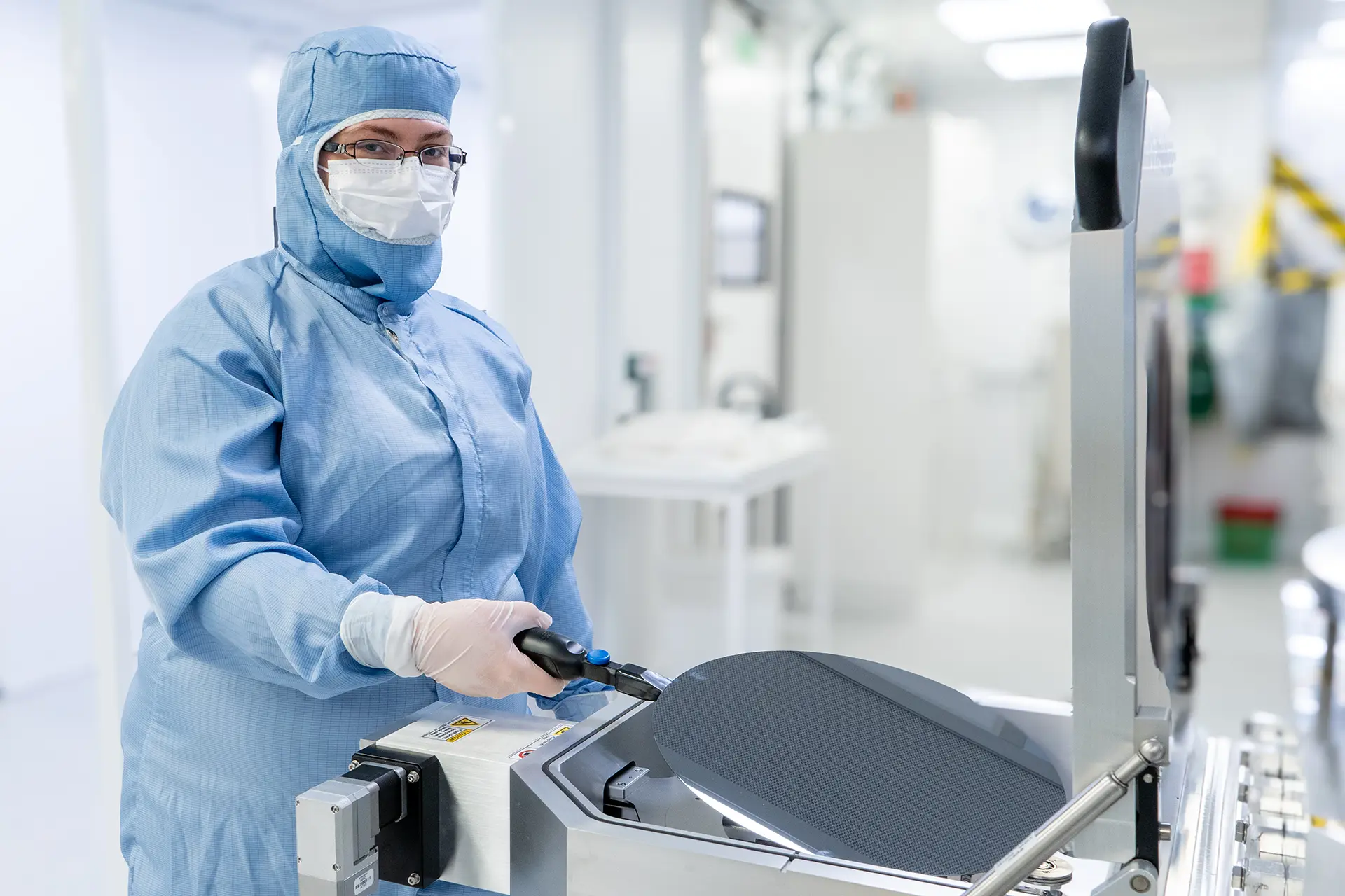
AlixLabs set out to rewrite this equation with Atomic Layer Etch Pitch Splitting (APS™): a breakthrough ALE process that delivers ultra-fine patterns without piling on costly EUV steps and multi-patterning complexity.

We backed AlixLabs at seed when APS was a lab-scale demonstration and the industry still treated ALE pitch splitting as a curiosity. We invested to help the team prove their process on real wafers, under real fab constraints, and build a business around it.
Since then, we’ve continued with additional capital in the Series A and support at board level. Arjan Göbel represents FORWARD.one on the board, bringing hardware and semicon equipment expertise into every strategic decision, from beta-tool roadmap to OEM engagement. We were chosen by CEO Jonas Sundqvist specifically for that hardware experience, and we use it to keep the company focused on one thing: getting APS adopted in high-volume manufacturing.


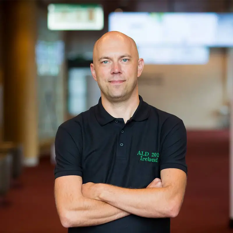
Dr. Jonas Sundqvist
Co-founder & CEO

Turning a scientific accident into a new scaling path: